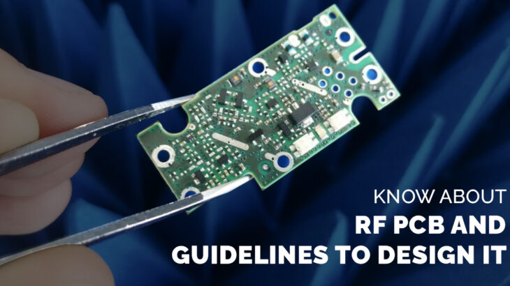
Radiofrequency refers to signals with high frequencies. Unlike PCB designs for low or line-frequency systems, RF PCB design distinguishes itself due to the challenges posed by the elevated frequencies that deviate from conventional guidelines. These RF PCB design guidelines are essential to follow in the PCB design services as they offer optimal methods for constructing circuit boards tailored to RF performance, considering factors such as signal integrity, dependability, effectiveness, and more. Hence, this blog will explore the preeminent strategies for achieving excellence in RF PCB design.
RF PCB Design:
An RF PCB refers to a printed circuit board which operates within the RF frequencies. Incorporating digital or analog devices within RF PCB design is feasible. The RF PCBs require a high-frequency process, necessitating an alternative PCB substrate material distinct from the conventional FR4. In the same way, the digital and analog components placed in RF PCBs offer mixed signal boards and should be integrated carefully to prevent integrity and signal problems for transmission.
RF PCBs are classified as low and high-power. Thus, RF PCB designing guidelines may undergo slight adjustments based on the frequencies and power.
RF PCB Design Guidelines:
The following are the guidelines to be considered in designing RF PCBs. They are,
Substrate Selection Of RF PCB:
RF PCBs are capable of managing frequencies ranging from low MHz to high GHz. The choice of PCB material holds significance in guaranteeing signal integrity, functional reliability, and high-frequency consistency. The elements to consider during the PCB material selection are,
- Thermal expansion coefficient (CTE)
- Dielectric constant
- Loss of tangent or dissipation
The common materials used for the RF PCB substrate are RO4000, RO3000, RT/Duroid, etc. It is essential that you choose copper material for RF PCB stack-up
Layer Stacking PCB:
The following are the key areas which should be given special attention in the RF PCB design stack-ups. They are,
- Spacing between the components
- Isolated traces
- Placing of components
- Layer count and arrangements
- Decoupling power supply
Within RF PCBs, the top layer contains the routing of RF traces, while the immediate layers are for power and ground planes. The ground plane in the immediate layer provides an optimal path for ground current return. The bottom layer is where non-RF traces are positioned and strategically arranged to mitigate any potential interference between non-RF and RF elements.
Trace Design For RF PCB:
RF PCB traces are susceptible to signal degradation and disturbances caused by interference. The primary focus in designing RF traces revolves around maintaining the correct characteristic impedance. Coplanar waveguides, striplines, and microstrips are the most commonly employed RF traces. When designing RF PCB traces, it’s essential to adhere to the following guidelines such as,
- Keep the traces at a minimum (short) to prevent attenuation.
- Avoid parallel placing of RF and non-RF traces as it may cause interference.
- Always place the test points outside the traces.
- The inclusion of curved ends improves the RF PCB performance.
Hence, these are the primary guidelines for designing RF PCB design. Approach Sunstream for PCB layout services for potential RF PCB board development.


 +1.585.935.7123
 +91-804-148-6861