
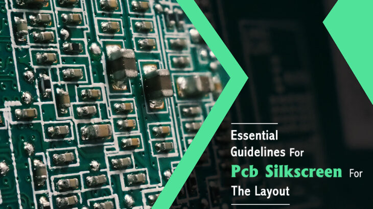
A layer of ink traces called a silkscreen is used to identify things like PCB pieces, warning signals, test points, logos, and marks. The silkscreen is often placed to the component side, although it is also customary to use silkscreen on the solder side. However, this can raise the price. In essence, a thorough PCB layout services in silkscreen can assist the engineer and the manufacturer in locating and identifying all the components.
It’s an epoxy non-conductive ink. These markings are made with carefully formulated ink. We typically see black, white, and yellow as the three primary hues. Standard fonts are also used by PCB software in silkscreen layers, although you have the option to select another font from the system. You need a polyester screen stretched on an aluminum surface for classic silk-screening.
Using a silkscreen, the following details can be displayed:
- Parts’ polarity;
- their location of parts using reference designators;
- Test point identification;
- Board-specific identification numbers;
- Warning symbols.
Basic understanding of the PCB silkscreen design:
Base Copper oz Minimum silkscreen width Silkscreen Height
(mil) (mil)
0.5 4 24
1 5 30
2 6 36
When it comes to PCB layout during the silkscreen stage, the design should adhere to the standard width/height ratio of 1:6, which may ensure that the silkscreen is displayed on the entire PCB board with a good resolution performance. This will be in regard to PCB design services, where we check through all the design attributes.
PCB silkscreen Design Rule;
W/H = 1/6
Where H = height, W = width.
The Process Of Silkscreen:
- The board is fixed to the printing device. The following four stages, appropriate for printing directions, involve the screen moving up, down, and left.
- To print the silkscreen on the PCB, the ready PCB (which has already been etched) is positioned beneath the silkscreen material. The silkscreen artwork on top of the PCB should line up precisely. Stoppers located at the PCB’s sides can be used to do this.
- Using a squeegee, Silkscreen UV curable ink is applied on top of the PCB. Dry for few minutes using a drying oven. Now the board should clearly display the text or marking.
Methods Of PCB silkscreen:
The PCB silkscreen process depends on several variables, including time, money, the level of precision needed, the amount of board space available, and the type of PCB material utilized. These characteristics have a reasonable trade-off for each approach outlined below to assist you in making PCB design decisions.
Manual screen printing – This is the oldest and most cost-effective PCB Silkscreen method. Its ease of setup and low setup costs make it a popular option. Additionally, due to its application, hand screen printing is still a desirable alternative for many projects.The registration tolerance is 0.005″ or line widths are greater than 0.007″

 +1.585.935.7123
 +91-804-148-6861